Research Stories
Direct Patterning of Colloidal Quantum Dots
with Adaptable Dual-ligand Surface
Development of ultra-high-resolution quantum dot (QD) patterning technology that could be implemented in nearly all QD photonic applications.
SKKU Advanced Institute of Nano Technology
Prof.
BAE, WANKI
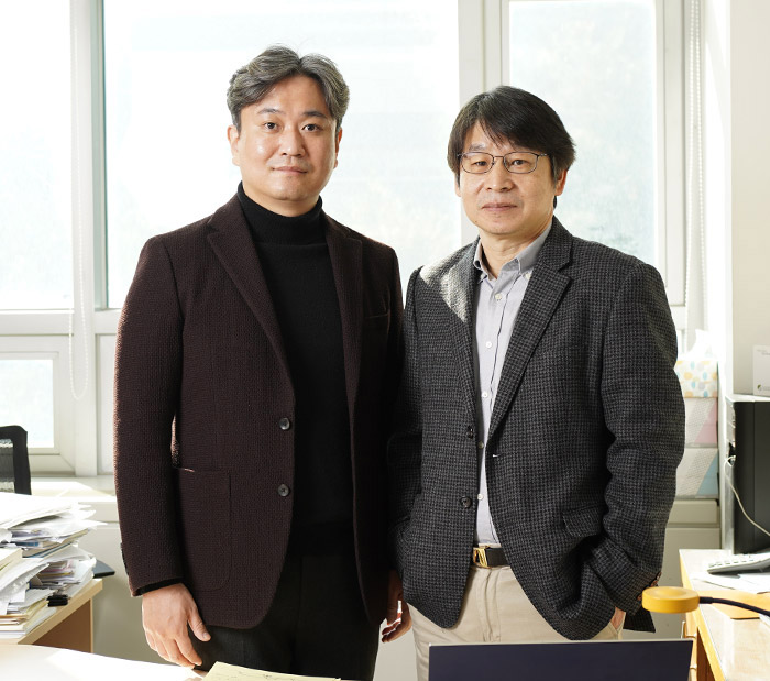
Researcher Donghyo Hahm, Researcher Jaemin Lim
A joint research team from SKKU (Prof. Wan Ki Bae), Sogang University (Prof. Moon Sung Kang), and Electronics and Telecommunications Research Institute (Dr. Chan-mo Kang) have developed ultra-high-resolution quantum dot (QD) patterning technology that could be implemented in nearly all QD photonic applications. The study appears in the journal ‘Nature Nanotechnology’ in August.
QDs are a new class of luminophores that stand at the forefront of nearly all light-emitting applications. The success of next-generation QD displays demands multicolor QD patterns on desired substrates over a large area with high-precision and high-definition, and most importantly, without compromising on optical or optoelectronic characteristics of QDs.
Here, the researchers devise QD materials that can be processed via photolithographic processes without the presence of photoresists and photoinitiators. Specifically, the researchers devise a dual-ligand passivation system comprising photocrosslinkable ligands (PXLs) and dispersing ligands (DLs) to enable QDs to be universally compatible with solution-based patterning techniques.
Upon UV irradiation, PXLs create a covalent bond between the ligands of neighboring QDs. The chemically crosslinked QD films are no longer dispersible when a solvent is applied. Hence, the researchers can achieve QD patterns by selective UV irradiation on QD films followed by development with good solvents.
The dual-ligand passivation system awards full freedom to choose the solvent, and thus the processing
methods. The dual-ligand passivation approach does not demand extra processing steps besides standard microfabrication processes, promising its immediate and practicable use in a range of photonic applications across academia to industry.
The highlight of the present work is the demonstration of high-definition, large-area QD patterns via commercialized photolithography (i-line) or inkjet printing techniques at no cost to the optical properties of QDs or optoelectronic performances of devices implementing them. As an ultimate achievement, the researchers exemplify the integration of bright, multicolored QD patterns attained by the present approach into optoelectronic devices.
For the “mixed-reality” (i.e., virtual reality and augmented reality) applications, the QD deposition process should enable the patterning of RGB QDs (or RG QDs along with the blank) into a few micrometer sub-pixels over a large area with high-precision and high-fidelity. The advantages of the present approach are well represented by the high-definition QD patterns over a large area achieved by means of standard photolithography equipment (i.e., pixel resolution for primary colors over 15,000 ppi on a 6-inch wafer)
Our approach offers a versatile way of creating various structures of luminescent QDs in a cost-effective and non-destructive manner, and could be implemented in nearly all commercial photonics applications where QDs are used.
[Figure] Schematic illustration of dual-ligand QDs and multi-colored patterns made of direct patterning of dual-ligand QDs
[Reference] Donghyo Hahm, Jaemin Lim, Hyeokjun Kim, Jin-Wook Shin, Sungkwon Hwang, Seunghyun Rhee, Jun Hyuk Chang, Jeehye Yang, Chang Hyeok Lim, Hyunwoo Jo, Beomgyu Choi, Nam Sung Cho, Young-Shin Park, Doh C. Lee, Euyheon Hwang, Seungjun Chung, Chan-mo Kang, Moon Sung Kang, and Wan Ki Bae, Direct patterning of colloidal quantum dots with adaptable dual-ligand surface, Nature Nanotechnology, 10.1038/s41565-022-01182-5
[Main Author] Wan Ki Bae (SKKU), Moon Sung Kang (Sogang University), Chan-mo Kang (Electronics and Telecommunications Research Institute), Donghyo Hahm (SKKU), Jaemin Lim (SKKU), Hyeokjun Kim (Sogang University)
* Contact: Prof. Wan Ki Bae (wkbae@skku.edu), Prof. Moon Sung Kang (kangms@sogang.ac.kr), Dr. Chan-mo Kang (nkcm@etri.re.kr)


