Development of fish skin-derived composite material-based bioinks and porous collagen bioinks
School of Medicine/Department of Precision Medicine, Prof. GeunHyung Kim, SeoYul Jo, YoungWon Koo
Medicine KIM, GEUNHYUNG Prof. · SeoYul Jo, YoungWon Koo

-
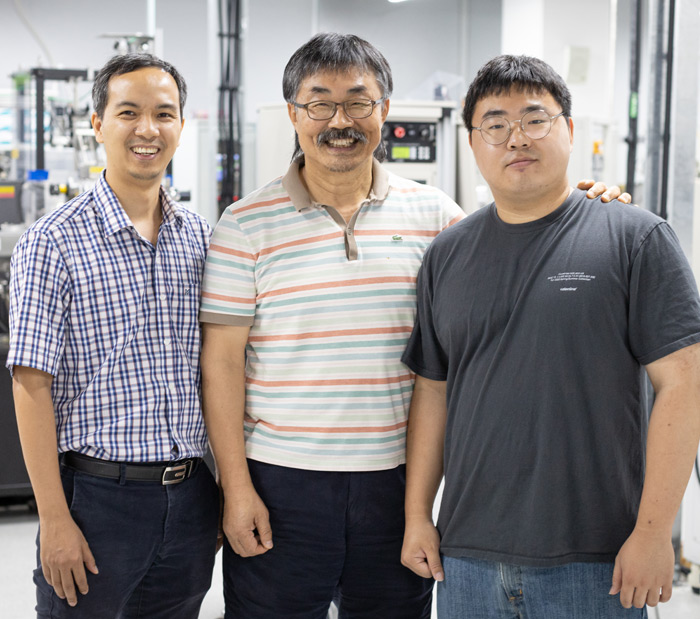
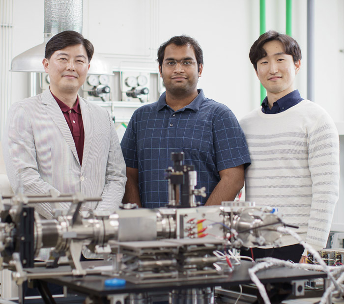
Center for Integrated Nanostructure Physics LEE, YOUNGHEE Prof. ·Researcher Van Luan Nguyen, Researcher Dinh Loc Duong, Researcher Sang Hyub Lee
How to Stack Graphene up to Four Layers
Graphene, an atomically thin hexagonal structure of carbon atoms is a potential candidate for electronic and optoelectrical applications such as transparent electrodes and interconnect for integrated circuits. Yet, it is one thing to possess such useful properties and to induce an intended characteristic from this “wonder material” is another. In the face of the end of the “Moore’s Law”, chip makers have set their sight on multi-layered graphene for its scaling ability of integrated circuits to smaller physical dimensions and the electric-field induced bandgap, which is not affordable in monolayer graphene. Furthermore, owning to exotic physical properties controlled by its stacking orders (the arrangement of graphene layer along vertical direction) such as superconductivity and quantum Hall effect to name a few, multilayer graphene is an interesting material for condensed matter physicists. for its extreme conductivity and stability. Still, the unknown growth method for uniform single-crystalline multilayer graphene growth in a wafer scale presents a challenge. Led by professor LEE Young Hee at the Center for Integrated Nanostructure Physics, the Institute for Basic Science (IBS) in Sungkyunkwan University, South Korea, an IBS research team reports a novel method to grow multi-layered, single-crystalline graphene with a selected stacking order in a wafer scale. Moreover, the research team could arrange a full multilayer graphene film along the right vertical direction without no sticking points, meaning that they can feature ***** . They obtained four-layered graphene using chemical vapor deposition (CVD) via Cu-Si alloy formation. There have been several approaches to control the number of graphene layers. Conventionally, the monolayer graphene, which is easily grown on Cu-substrate, can be detached from the Cu-substrate and transferred onto insulator substrates such as SiO2/Si. Therefore, the simplest method to make multilayer graphene is to stack them layer-by-layer via the transfer process. However, this transfer process may cause tearing, wrinkles, and/or polymer residues. Though such issues can be avoided via a direct method, i.e. CVD on Cu substrate, the low solubility of carbon (C) in copper (Cu) hampers the controlling of the number of graphene layers with high uniformity in a large area. By depositing Ni or Co to form Cu-Ni/ Cu-Co alloys or employing oxygen-rich Cu substrate, C solubility in Cu is boosted and thus stacks more layers of graphene. Nevertheless, a small portion of inhomogeneous multilayers occurs. Controlling the crystallographic stacking sequence of graphene films thicker than two layers with high uniformity has not been demonstrated to date. Figure 1. Schematic of growth process. Step I: Si atoms were uniformly distributed in the monocrystalline Cu(111) film; step II: SiC formation at 900 ℃ in a H2-rich environment; step III: multilayer graphene islands were grown at 1075 ℃; step IV: a full multilayer graphene film was obtained. Dr. Van Luan Nguyen, the first author of the study (now at Samsung Advanced Institute Technology) proposed to use silicon carbide (SiC) on the surface of Cu substrate alloy, via the sublimation of Si atoms at a high temperature. They controlled the C solubility in the Cu film by introducing Si content on Cu surface by heat treatment of Cu substrate with a constant H2 gas flow inside the quartz tube of CVD chamber. “The formation of a homogeneous Cu-Si alloy, as a role of catalyst, was critical to control the number layers of graphene film in a wafer scale with methane gas. With the presence of Cu-Si alloy, SiC can be formed when methane gas is injected and the following sublimation process of Si atoms leaves C atoms behind to form multilayer graphene. Si amount is fixed at 28.7 % for uniform multilayer graphene film. Depending the concentrations of argon (Ar)-diluted methane gas, the number of graphene layers varies,” says Dr. Van. Figure 2. Optical micrographs of mono-, bi-, tri-, and tetralayer graphene on the SiO2/Si substrate. The insets of show cross-sectional TEM images of the corresponding graphene films. Figure 3. Photograph of centimeter-scale mono-, bi-, tri-, and tetralayer graphene on the SiO2/Si substrate. “Growing in a large scale of this much-hyped graphene has seen much progress over a decade, but building multi-layered graphene is just in its early stages. Our study offers a novel approach to upgrade the conventional CVD method by introducing an intermediate process of in-situ formation of SiC film,” notes Dr. LEE Sang Hyub, coauthor of the study. Importantly, this study provides a new platform to synthesize graphene multilayer towards the uniform large-area single-crystalline layer-tunable multilayer graphene as well as graphite thin film. This is an initial step to incorporate multilayer graphene to display panels and integrated circuits such as via-holes and replacement of Cu electrodes as well as photo-electronic and photovoltaic devices. “Deposition of Si by conventional methods at low temperatures such as thermal evaporation or sputtering does not work for uniform multilayer graphene growth. The key in our new approach is to form uniform Cu-Si alloy on quartz tube chamber in which Si is sublimated at high temperature of 900 ℃ with H2 gas flow in a controllable manner,” explains Director LEE Young Hee, the corresponding author of the study. Although the substantial achievement has been demonstrated in our current work, Director Lee cautions that the method to deposit Si at high temperature during the growth process is not practical and can be harmful for the quart tube for long-term use. They are searching for a solution to replace the current one for mass product.
- No. 141
- 2020-08-18
- 4095
-
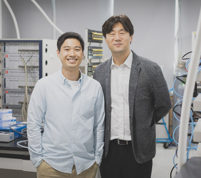
Semiconductor Systems Engineering CHOI, JAE HYUK Prof. ·Prof. Jung-Hoon Chun·Researcher Hyeong-Seok Seo
Development of the nation’s first CMOS LiDAR Sensor System-on-Chip
Prof. JaeHyuk Choi and Prof. Jung-Hoon Chun in the Department of Semiconductor Systems Engineering at SKKU have successfully developed the nation’s first CMOS Light Detection and Ranging (LiDAR) sensor for autonomous vehicles. The research paper was presented at the VLSI symposia, the top-tier conference on semiconductor circuits and technologies. Founded in 1981, VLSI symposia has a 40-year history this year and is one of the most prestigious conferences. It is also well known for selecting papers through a rigorous review process and for leading companies such as Intel and Samsung to present the latest technology competitively. A LiDAR sensor measuring a distance of objects as well as 2-dimensional shape is an essential component for object/environment detection and recognition in autonomous vehicles, robots, and drones. Even though several LiDAR sensors were already commercialized, these products have the large form factor and high price owing to the assembly of many discrete IC components. The SKKU’s LiDAR sensor that is a single semiconductor chip with 6 x 5 mm2 size offers mass production with low-cost semiconductor (CMOS) technology. Several CMOS LiDAR sensors were already presented by overseas companies and research institutes such as Toshiba, Toyota, and EPFL. SKKU developed the first CMOS LiDAR sensor in Korea. More importantly, SKKU addressed two critical problems of inter-LiDAR interference between multiple vehicles and performance degradation according to weather conditions. SKKU newly developed an interference filter and a multi-event histogramming time-to-digital converter to provide reliable detection up to 48m range in real road applications where many vehicles run simultaneously. In collaboration with domestic companies, SOS Lab and Samsung Electronics, our research team successfully developed prototype sensor chips and outperformed existing LiDAR sensors. SKKU presented the paper at the VLSI symposia's Image Sensor and Imaging Techniques session in June 2020. A total of 5 papers presented in the session are mainly published by the world's top companies such as Samsung and Toshiba. Additionally, SKKU is the only domestic university that presented one of the five papers. ※Paper: “A 36-channel SPAD-integrated scanning LiDAR sensor with multi-event histogramming TDC and embedded interference filter”, Symposia on VLSI Circuits, 2020. ※Authors: Hyeongseok Seo (1st author, dept. of electrical and computer engineering, SKKU), Jaehyuk Choi (corresponding author, dept. of semiconductor systems engineering, SKKU), Jung-Hoon Chun (co-author, dept. of semiconductor systems engineering, SKKU), Heesun Yoon·Dongkyu Kim (co-authors, SOS Lab), Jungwoo Kim (co-authors, Samsung Electronics), Seong-Jin Kim (co-authors, dept. of electrical and computer engineering, UNIST)
- No. 140
- 2020-08-05
- 3540
-
Energy Science OH, SANG HO Prof. ·PhD. LEE, SU BIN
Nanoindentation processes in full view via in-situ TEM reveal the dislocation nucleation mechanism
The microelectronics revolution is one of the most influential drivers of current industrial developments. To probe the mechanical properties of ever shrinking materials and components, nanoindentation has come to be an omnipresent and indispensable method. In a recent combined experimental and computational approach, Prof. Sang Ho Oh was able to resolve the dynamic atomistic processes taking place at the elastic-plastic transition during nanoindentation for the first time. Further, Prof. Oh could determine the rate limiting processes governing the so-called pop-in event, as well as the origins for the observed transitions in dislocation mechanisms succeeding this event based on the dynamics of so-called prismatic dislocation loops. In the future, these fundamental insights will enable modifications of established nanoindentation models in order to better describe the most common small scale mechanical characterization technique. The research result was published on May 12 in Nature Communications (IF 11.880), an international science journal. Full details can be found in this open access article: In-situ observation of the initiation of plasticity by nucleation of prismatic dislocation loops S. Lee et al, Nature Communications, published 05/12/2020 https://doi.org/10.1038/s41467-020-15775-y [Fig. 1] Formation of shear loops during plastic deformation. From the real-time transmission electron microscopy nanoindentation transformation experiment of gold nanowires, the experimental results and atomic simulation results of observing the formation process of dislocation loops during the initial plastic deformation process
- No. 139
- 2020-07-20
- 3271
-
Energy Science YOON, WON SUB Prof. ·Researcher Eunkang Lee
Provides a new way to develop cathode materials for longer and safer vehicle batteries
Prof. Won-Sub Yoon’s research team successfully derives the key factors on the thermal instability of Ni-rich cathode material for lithium-ion batteries. This research work was published in the Advanced Science (IF: 15.804) on April 24 as a back cover, with the title "Tracking the Influence of Thermal Expansion and Oxygen Vacancies on the Thermal Stability of Ni‐Rich Layered Cathode Materials." The extensive demand for high energy storage in electric devices, electric vehicles and smart grid systems has led to the commercialization of rechargeable lithium ion batteries using Ni-rich layered cathode material. Simultaneously, the safety issue from the thermal instability of Ni-rich cathode materials has been introduced. Until now, the strategy to enhance its thermal stability has been approached based on fragmentary facts that the thermal instability is merely attributed to the thermally unstable Ni element. However, these approaches have limitations in providing a custom solution to the fundamental cause of thermal instability involving Ni element. Prof. Won-Sub Yoon's research team showed that the thermal expansion of Li slab become larger as the increase of Ni content in the cathode material before the onset temperature of layered to disordered spinel phase transition is reached. This thermal expansion of Li slab induces the elongation of intermediate tetrahedron in pathway of cation migration, resulting in an expanded pathway with a low energy barrier for cation migration. In addition, the oxygen vacancies are formed and accumulate around only Ni ions before the onset temperature of phase transition is reached. In presence of oxygen vacancies, the cation migration pathway is energetically mitigated as Ni ion migrates through the face-shared oxygen plane that does not contain oxygen vacancies. Herein, the team proposed the thermal expansion and oxygen vacancies as new critical factors to affect thermal stability of charged Ni-rich cathode materials as shown in the figure below. [Figure 1] Occurrence of thermal expansion and oxygen vacancies in Ni-rich layered cathode materials due to increase of temperature and the process of change in the crystal structure and phase transition ※ Title: Tracking the Influence of Thermal Expansion and Oxygen Vacancies on the Thermal Stability of Ni‐Rich Layered Cathode Materials ※ Original Article URL: https://onlinelibrary.wiley.com/doi/full/10.1002/advs.201902413
- No. 138
- 2020-07-06
- 4022
-
Mechanical Engineering KIM, JAEHOON Prof. ·Researcher Handi Setiadi Cahyadi
Revealing the Intercalation Mechanisms of Lithium, Sodium, and Potassium in Hard Carbon
Revealing the Intercalation Mechanisms of Lithium, Sodium, and Potassium in Hard Carbon Due to its high stability, widespread availability, low-cost, and excellent performance, hard carbon is considered as one of the most promising anode materials for sodium and potassium-ion batteries. To further develop a high-performance electrode, it requires a deep understanding of the carrier-ion storage mechanism. However, this has proven to be not such a trivial task because of the complex structure of hard carbon. Recent work by Prof. Kim and his team unveil that the sloping voltage region is caused by the adsorption of Li-ion, Na-ion, and K-ion on the surface of active sites such as defects, edges, and residual heteroatoms. Afterward, the carrier-ions penetrate into the graphitic layers, creating a low voltage plateau region. This finding also further proven by DFT simulation, which revealed the change in the inner molecular structure of the hard carbon during the discharge process. The “ripening” phenomenon, in which the edge of the hard carbon structure open up when the carrier ion approach to the edge of graphitic layer, is very prevalent for the Na-ion and K-ion because of their larger electronic radius. However, the same degree of ripening does not occur for the Li-ion, which leads to a smaller capacity as compared to the Na-ion and K-ion. This finding is a breakthrough that will help future researchers understand the ion-storage mechanism behind the hard carbon material. In addition, the underlying concept of “ripening” phenomenon can be used to develop a high-performance electrode material in the future. This research was supported by the Technology Development Program to Solve Climate Changes of the National Research Foundation (NRF) funded by the Ministry of Science, ICT & Future Planning (2017M1A2A2087635) and the Waste‐to‐Energy Technology Development Program of the Korea Environmental Industry & Technology Institute with financial resources provided by the Ministry of Environment, Republic of Korea (No. 2018001580001). This research was published in 'Advanced Energy Material' on April 15. ※ Title : Intercalation Mechanisms: Revealing the Intercalation Mechanisms of Lithium, Sodium, and Potassium in Hard Carbon ※ Source : https://onlinelibrary.wiley.com/doi/abs/10.1002/aenm.202000283 This diagram demonstrates the electron radius of ions and hard carbon's layer and its transposition when Li, Na, and K ions are inserted into hard carbon. The K- ions with the largest electron radius show the broadest edge expansion in which subsequent K- ions can penetrate deeper into the inter layer spacing of hard carbons.
- No. 137
- 2020-06-19
- 3809
-
Mechanical Engineering BAIK, SEUNGHYUN Prof. ·Prof. Hyungpil Moon, and Prof. Moon Ki Kim
Develops Highly Conductive Healable Nanocomposite Materials
Prof. Seunghyun Baik, Prof. Hyungpil Moon, and Prof. Moon Ki Kim from SKKU’s School of Mechanical Engineering made a research report about the highly conductive completely reversible electron tunneling-assisted percolation network of silver nanosatellite particles for putty-like moldable and healable nanocomposites. Prof. Daewoo Suh (School of Mechanicl Engineering) and Prof. K. P. Faseela (Dept. of Energy Science) are co-first authors on the report. □ Deformable and healable conductive materials have received considerable attention due to their use in emerging future electronics, such as artificial human skin, internet of things, and bioelectronics, owing to their ability to recover from mechanical/electrical damage. However, their practical applications have been impeded by low electrical conductivity and irreversible conductivity degradation after breaking/healing cycles. □ The research team’s report is about the development of a highly conductive completely reversible electron tunneling-assisted percolation network of silver nanosatellite particles for putty-like moldable and healable nanocomposites. The densely and uniformly distributed silver nanosatellite particles with a bimodal size distribution are generated by the radical and reactive oxygen species-mediated vigorous etching and reduction reaction of silver flakes using tetrahydrofuran peroxide in a silicon rubber matrix. The close work function match between silicone and silver enables electron tunneling between nanosatellite particles, achieving high electrical conductivity and ~100% electrical healing efficiency. □ As an application demonstration, the highly conductive putty-like nanocomposites are employed as random-shaped electrical interconnectors, stably operating light-emitting diodes. An emergency electronics repair demonstration was also performed by a robot using the team’s nanocomposites. □ The research was published in Nature Communications. Daewoo Suh, K. P. Faseela, Wonjoon Kim, Chanyong Park, Jang Gyun Lim, Sungwon Seo, Moon Ki Kim, Hyungpil Moon, Seunghyun Baik, Electron tunneling of hierarchically structured silver nanosatellite particles for highly conductive healable nanocomposites, Nature Communications, 11, 2252 (May 2020), https://doi.org/10.1038/s41467-020-15709-8 Hierarchically structured silver nanosatellite particles for the highly conductive, moldable, healable, and stable nanocomposites.
- No. 136
- 2020-06-01
- 3907
-
Chemical Engineering KIM, JUNG KYU Prof. ·Byong Wan Lee(SKKU postgraduate)
Prof. Kim Introduces Highly Efficient Solar-Hydrogen Energy Technology with the Plasmonic Patterned Structure of Au NSS
Prof. Jung Kyu Kim (School of Chemical Engineering) reported his research achievement: development of a novel transfer-printing of highly ordered Au nanosphere array to enhance light absorptance, charge transport and charge transfer performance of metal oxide films and their application for the photoanode of photoelectrochemical solar water splitting with high efficiency. N‐type metal oxides such as hematite (α‐Fe2O3) and bismuth vanadate (BiVO4) are promising candidate materials for efficient photoelectrochemical water splitting; however, their short minority carrier diffusion length and restricted carrier lifetime result in undesired rapid charge recombination. Herein, a 2D arranged globular Au nanosphere (NS) monolayer array with a highly ordered hexagonal hole pattern (hereafter, Au array) is introduced onto the surface of photoanodes comprised of metal oxide films via a facile drying and transfer‐printing process. Through plasmon‐induced resonance energy transfer, the Au array provides a strong electromagnetic field in the near‐surface area of the metal oxide film. The near‐field coupling interaction and amplification of the electromagnetic field suppress the charge recombination with long‐lived photogenerated holes and simultaneously enhance the light harvesting and charge transfer efficiencies. Consequently, an over 3.3‐fold higher photocurrent density at 1.23 V versus reversible hydrogen electrode (RHE) is achieved for the Au array/α‐Fe2O3. Furthermore, the high versatility of this transfer printing of Au arrays is demonstrated by introducing it on the molybdenum‐doped BiVO4 film, resulting in 1.5‐fold higher photocurrent density at 1.23 V versus RHE. The tailored metal film design can provide a potential strategy for the versatile application in various light‐mediated energy conversion and optoelectronic devices. This research outcome was published on 24th, April, 2020 in ‘Advanced Energy Materials’ (IF: 24.88), a world-renowned scientific journal. *Original Article: Retarded Charge–Carrier Recombination in Photoelectrochemical Cells from Plasmon‐Induced Resonance Energy Transfer, Advanced Energy Materials, https://onlinelibrary.wiley.com/doi/full/10.1002/aenm.202000570 *The researchers : Byoung Wan Lee (First Author, SKKU postgraduate), Jung Kyu Kim (Corresponding Author, Professor, School of Chemical Engineering)
- No. 135
- 2020-05-19
- 3740
-
Biomedical Engineering WOO, CHOONG-WAN Prof. ·Lada Kohoutová Researcher
Opening a black box: Interpretation of machine learning models in neuroimaging
□ Neuroimaging allows us to gain huge amount of data of the brain structure and function, and these data need to be processed with sophisticated methods. Machine learning has gained a large popularity in this field as a tool with which it is possible to create computational models of the brain function related to behaviour or cognitive stimuli. However, these models are complex and often an unreadable “black box” to humans. A computational model of the brain, in which we cannot explain why and how it works, only hardly contributes to the neuroscientific knowledge or clinical practice. Itis, thus, necessary to develop interpretation methods of such models. □ In the Cocoan lab (https://cocoanlab.github.io) lead by Choong-Wan Woo (Center for Neuroscience Imaging Research, Institute for Basic Science, Department of Biomedical Engineering, Sungkyunkwan University in South Korea), Lada Kohoutová (PhD student) and colleagues developed a framework of model interpretation and on its basis, they assembled a protocol according to which it is possible to easily assess and interpret a model from the aspect of its behaviour, significant features and in the context of biology (Fig. 1). Individual steps of their analysis pipeline yield a number of component results that together create an interpretable picture of a model. They introduced the framework along with the protocol in an article published in the journal, Nature Protocols. □ Prof. Choong-Wan Woo, who led the study, said, "Machine learning and the use of artificial intelligence are becoming more and more popular and common in various fields of neuroimaging, and thus the need for interpreting and explaining neuroimaging-based machine learning models is rapidly increasing,” and added, "This study will help develop neuroimaging-based predictive models that can be explained and trusted, and further promote a deeper understanding of brain mechanisms and its disorders” □ Lada Kohoutová, the first author also said, “Methods and procedures of interpreting machine-learning models in neuroimaging are not yet well-established and unified. Our protocol aims to establish a basis for a unified approach to model interpretation, open this black box a little, and so contribute to a deeper understanding of the brain and its function.” □ This work was supported mainly by Institute for Basic Science (IBS-IBS-R015-D1), National Research Foundation (2019R1C1C1004512), Ministry of Science and ICT (18-BR-03 and 2019-0-01367-BabyMind). □ This work is published in Nature Protorcols (IF 11.334) on March 18, 2020. ※ For video abstract, please visit https://youtu.be/kcDfEkoQa7Y
- No. 134
- 2020-04-27
- 4383
-
Mechanical Engineering KIM, TAESUNG Prof. ·Dr. KIM, Hyeong-U
Metallic 1T, Using Plasma-enhanced Chemical Vapor Deposition (PECVD), Film Synthesis Technique Developed
School of Mechanical Engineering/SAINT Prof. Kim, Taesung‧ Dr. Kim, Hyeong-U Development of New Method for Synthesis of Stable 1T-WS2 using PE-CVD Prof. Taesung Kim in Mechanical Engineering/SAINT and Dr. Hyeong-U Kim in SAINT have developed the synthesis technique of various 2-dimensional (2D) material using plasma-enhanced chemical vapor deposition (PECVD). A related research paper, ‘Wafer-scale of 1T-WS2 film for efficient and stable hydrogen evolution reaction.’ was published and featured on the back cover of ‘Small’ (IF: 10.85, JCR <10%). Professor Kim’s group reported the synthesis of large-scale MoS2 which is one of the typical transition metal dichalcogenides (TMDs) using PECVD at low temperature (<150 oC) for the first time in the world (Advanced Materials, 2015). Furthermore, a metal oxide group, α-MoO3 (Nanotechnology, 2017) and MoS2-Graphene heterostructure (Applied Surface Science, 2019) were synthesized for various applications. As 1T-phase WS2 (1T-WS2) typically has meta-stable structure with metallic properties, which can lead to excellent electrochemical catalytic properties as alternative materials for platinum, Prof. Taesung Kim group and Prof. Jae-Hyun Lee (Ajou University) group worked for the synthesis of stable 1T-WS2 with nano grain size for application of hydrogen evolution reaction (HER). The plasma can generate a nano grain size of 1T-WS2 with high surface energy so it can be stable in atmospheric pressure and room temperature. It was stable with 1,000 cycles and 1 month of exposure in the air for HER. Professor Kim mentioned that PECVD enables the wafer-scale synthesis of stable 1T-WS2 with high uniformity at low temperature (<150 oC) and this can be one of the critical technologies for future Hydron energy industry. (Currently, Dr. Hyeong-U Kim continues his research career at Northwestern University under the guidance of Professor Mark C. Hersam working on the synthesis of TMDs using MOCVD for memristor application.) ※ Related Papers 1) Low-Temperature Synthesis of Large-Scale Molybdenum Disulfide Thin Films Directly on a Plastic Substrate Using Plasma-Enhanced Chemical Vapor Deposition (Advanced Materials, 27, 2015, 5223-5229) (First Author: Dr. Chisung Ahn / Corresponding: Prof. Changgu Lee, Prof. Taesung Kim) 2) Highly uniform wafer-scale synthesis of α-MoO3 by plasma-enhanced chemical vapor deposition (Nanotechnology, 28, 2017, 175601) (First: Dr. Hyeong-U Kim / Corresponding: Prof. Taesung Kim) 3) Low-temperature wafer-scale growth of MoS2-graphene heterostructures (Applied Surface Science, 470, 2019, 129-134) (First: Dr. Hyeong-U Kim / Corresponding: Prof. Jae-Hyun Lee, Prof. Taesung Kim) 4) Wafer-Scale and Low-Temperature Growth of 1T-WS2 Film for Efficient and Stable Hydrogen Evolution Reaction (Small, 16, 2020, 1905000) (First: Dr. Hyeong-U Kim, Vinit Kanade, Mansu Kim / Corresponding: Prof. Jae-Hyun Lee, Prof. Taesung Kim) ○ Prof. Taesung Kim (Corresponding author), Dr. Hyeong-U Kim (1st author)
- No. 133
- 2020-04-14
- 3939
-
Energy Science YANG, HEEJUN Prof.
Quantum Mechanical Interlayer Interaction for Energy-Efficient 2d Vertical Transistors
Prof. Yang’s group (with Dr. Shoujun Zheng) recently reported the development of a new conceptual tunneling transistor based on resonant tunneling and the Stark effect in 2D heterostructures, which can operate with 100 times less energy consumption in comparison to conventional silicon devices. Recently, vertical tunneling transistors have demonstrated smaller subthreshold swing (SS) than silicon-based transistors. The 60 meV SS value of silicon devices has been considered the ultimate limit for transistors. However, inevitable thermal energy and non-resonant tunneling phenomena have prevented the development of practical tunneling transistors based on 2D materials. Prof. Yang’s research showed that the quantum mechanical Stark effect could resolve the issue in atomically thin tunneling transistors. The Stark effect was discovered in 1914, and as a result Johannes Stark was awarded the Nobel Prize in Physics in 1919. However, there has been no experimental verification of this effect at the device scale. In Prof. Yang’s study, the Stark effect was first observed at the device scale. Moreover, traditional phonons or excitons could be completely removed in transistor operation, which enabled a precise design of the tunneling transistors with a resolution of 0.01 eV. Prof. Yang mentioned that the tunneling transistor would be able to replace the key element in semiconductor technology, the field-effect transistor. This research was published in Advanced Materials (IF=25.809) on February 6, 2020. [Image] Resonant tunneling transistor based on 2Dmaterials and the corresponding band alignment of the materials
- No. 132
- 2020-03-27
- 3505
-
Chemical Engineering PANG, CHANGHYUN Prof. ·천성우 박사
Development of Triboelectric Energy Device Technology to Efficiently Harvest Horizontal Force-Based Energy
Despite the high-performance energy generation capabilities of previously reported triboelectric generator (TENG) devices, sensitive and efficient energy harvesting under contact/noncontact horizontal forces induced by in-plane stimuli is highly desirable for realizing portable and wearable electronics. Prof. Changhyun Pang in the Department of Chemical Engineering at Sungkyunkwan University (SKKU) reported on the versatile strategy for harvesting in-plane stimuli in TENG devices. A related research paper was published on the cover of Advanced Materials (Impact Factor 25.809). For wearable device applications that can be incorporated into cloth fabrics, accessories (watches, eyeglasses, etc.), and human skin, the power source is a crucial issue for long-term sustainable operation. The periodic recharging and exchanging of primary batteries causes maintenance time and costs. In this reason, Energy harvesting technology is considered an alternative solution to the power supply issue. In particular, a nanogenerator based on the triboelectric effect of two separated layers has been proven to be effective in utilizing irregular mechanical energy that is abandoned in everyday life. The architecture of a triboelectric nanogenerator (TENG) is mostly responsive to vertical pressure that leads to the contact of two separated layers. However, the efficient and sensitive generation of energy is not limited to the vertical direction. For example, in human body motion, friction as an energy generation source is mostly caused by a horizontal rubbing motion. So far, there has not been a pragmatic strategy to harvest the motion energy from various directions. The Pang’s team suggested a versatile strategy for TENG to transform in-plane kinetic energy into electricity. The assembled hairy-structures on the conventional TENG devices converts in-plane sliding motions into vertical vibration-like friction. This phenomena is due to momentary stress relief in transition between each of the pillars. Furthermore, the researchers also demonstrated that the microstructure is effective in capturing noncontact airflow due to the formation of dynamic vortices. This work showed an energy harvesting strategy that could be used for future wearable devices. Paper S. Chun, C. Pang, S. B. Cho, A Micropillar-Assisted Versatile Strategy for Highly Sensitive and Efficient Triboelectric Energy Generation under In-plane Stimuli, 32, 1905539, 2020.
- No. 131
- 2020-03-16
- 3522
-
Chemistry LEE, HYOYOUNG Prof.
Addressing Global Warming with New Nanoparticles and Sunshine
Press Release www.ibs.re.kr For immediate release Publication Information - Paper Title: Highly Efficient Nanostructured Metal-decorated Hybrid Semiconductors for Solar Conversion of CO2 to Absolute CO Selectivity - Journal, Publication Date: Materials Today, January 3, 2020 - Authors: Chau T. K. Nguyen, Ngoc Quang Tran, Sohyeon Seo, Hee Min Hwang, Simgeon Oh, Jinsun Lee, Jianmin Yu, Thi Anh Le, Joseph Hwang, Meeree Kim, Hyoyoung Lee - DOI: 10.1016/j.mattod.2019.11.005 - Contact Regarding this Press Release: Professor Hyoyoung Lee (hyoyoung@skku.edu), Mr. Kyungyoon Min, Head of IBS Communications Team (+82-42-878-8156, kymin@ibs.re.kr); or Ms. Dahee Carol Kim, Public Information Officer of IBS & Science Communicator (+82-42-878-8133, clitie620@ibs.re.kr) Addressing Global Warming with new Nanoparticles and Sunshine Artificial photosynthesis:visible-light-driven photocatalysts convert CO2 into oxygen and pure CO under water Harvesting sunlight, researchers of the Center for Integrated Nanostructure Physics, within the Institute for Basic Science (IBS, South Korea) published in Materials Today a new strategy to transform carbon dioxide (CO2) into oxygen (O2) and pure carbon monoxide (CO) without side-products in water. This artificial photosynthesis method could bring new solutions to environmental pollution and global warming. While, in green plants, photosynthesis fixes CO2 into sugars, the artificial photosynthesis reported in this study can convert CO2 into oxygen and pure CO as output. The latter can then be employed for a broad range of applications in electronics, semiconductor, pharmaceutical, and chemical industries. The key is to find the right high-performance photocatalyst to help the photosynthesis take place by absorbing light, convert CO2, and ensuring an efficient flow of electrons, which is essential for the entire system. Titanium oxide (TiO2) is a well-known photocatalyst. It has already attracted significant attention in the fields of solar energy conversion and environmental protection due to its high reactivity, low toxicity, chemical stability, and low cost. While conventional TiO2 can absorb only UV light, the IBS research team reported previously two different types of blue-colored TiO2 (or “blue titania”) nanoparticles that could absorb visible light thanks to a reduced bandgap of about 2.7 eV.[LD1] They were made of ordered anatase/disordered rutile (Ao/Rd) TiO2 (called, HYL’s blue TiO2-I) [LH2] (Energy & Environmental Science, 2016), and disordered anatase/ordered rutile (Ad/Ro) TiO2 (called, HYL’s blue TiO2-II) [LH3] (ACS Applied Materials & Interfaces, 2019), where anatase and rutile refer to two crystalline forms of TiO2 and the introduction of irregularities (disorder) in the crystal enhances the absorption of visible and infra-red light. [LD4] Figure 1. Proposed energy diagram representing the electron transfer mechanism in TiO2/WO3-Ag hybrid nanoparticles. This so-called Z-scheme shows the flow of charged particles (electrons, e- and holes, h+) through the different components of the nanoparticles. Blue TiO2 and WO3’s e- can occupy lower (valence band, VB) and higher (conductive band, CB) energy levels. Photons from sunlight (thunders) provide the energy for the e- to jump up from the VB to the CB (black arrows pointing upwards), leaving h+ behind. TiO2’s lower band is close, just a bit lower than WO3’s higher band level, so e- from the high band of WO3 can migrate to the VB of blue TiO2 to trap its holes. After separation, the excited e- jump from the CB of TiO2 onto silver nanoparticles allowing the conversion of CO2 into CO, while the photogenerated h+ in the WO3 site oxidize water (H2O) to form oxygen (O2). For the efficient artificial photosynthesis for the conversion of CO2 into oxygen and pure CO, IBS researchers aimed to improve the performance of these nanoparticles by combining blue (Ao/Rd) TiO2 with other semiconductors and metals that can enhance water oxidation to oxygen, in parallel to CO2 reduction into CO only. The research team obtained the best results with hybrid nanoparticles made of blue titania, tungsten trioxide (WO3), and 1% silver (TiO2/WO3–Ag). WO3 was chosen because of the low valence band position with its narrow bandgap of 2.6 eV, high stability, and low cost. Silver was added because it enhances visible light absorption, by creating a collective oscillation of free electrons excited by light, and also gives high CO selectivity. The hybrid nanoparticles showed about 200 times higher performance than nanoparticles made of TiO2 alone and TiO2/WO3 without silver. Starting from water and CO2, this novel hybrid catalyst produced O2 and pure CO, without any side products, such as hydrogen gas (H2) and metane (CH4). The apparent quantum yield that is the ratio of several reacted electrons to the number of incident photons was 34.8 %, and the rate of reacted electrons 2333.44 μmol g−1h−1. The same measurement was lower for nanoparticles without silver (2053.2 μmol g−1h−1), and for nanoparticles with only blue TiO2 (912.4 μmol g−1h−1). “We expect these results will help the industry-scaled CO2 reduction and produce oxygen and commercially available CO derivatives,” says Hyoyoung Lee, CINAP associate director. Figure 2. Efficient and selective production of CO with different nanoparticles. (a) The graph shows that hybrid TiO2/WO3-Ag (7BT/W1-A1) nanoparticles are the best at selectively producing pure CO, without H2 and CH4 side products within a 7-hour timeframe. These can be compared with nanoparticles made of blue TiO2, WO3, hybrid TiO2/WO3 (7BT/W1) and hybrid TiO2/Ag (W1-A1). (b) CO production using different hybrid nanoparticles made of TiO2/WO3-Ag (red lines), TiO2/WO3 (green lines) and TiO2-only nanoparticles (blue lines) within 9 hours. 7BT/W1-A1 with a concentration of 1% silver has the best performance. Notes for editors - References Kan Zhang, Luyang Wang, Jung Kyu Kim, Ming Ma, Ganapathy Veerappan, Chang-Lyoul Lee, Ki-jeong Kong, Hyoyoung Lee* and Jong Hyeok Park*, “An order/disorder/water junction system for highly efficient co-catalyst-free photocatalytic hydrogen generation”, Energy & Environmental Science, Energy & Environmental Science, 2016, 9, 499-503. Hee Min Hwang, Simgeon Oh, Jae-Hyun Shim, Young-Min Kim, Ansoon Kim, Doyoung Kim, Joosung Kim, Sora Bak, Yunhee Cho, Viet Q. Bui, Thi Anh Le and Hyoyoung Lee. Phase-Selective Disordered Anatase/Ordered Rutile Interface System for Visible-Light-Driven, Metal-Free CO2 Reduction, ACS Applied Materials & Interfaces. (2019). DOI: 10.1021/acsami.9b10837 Chau T. K. Nguyen, Ngoc Quang Tran, Sohyeon Seo, Hee Min Hwang, Simgeon Oh, Jianmin Yu, Meeree Kim, Thi Anh Le, Jinsun Lee, Hyoyoung Lee. Phase-Selective Highly Efficient Nanostructured Metal-decorated Hybrid Semiconductors for Solar Conversion of CO2 to Absolute CO Selectivity, Materials Today. DOI: 10.1016/j.mattod.2019.11.005 - Media Contact For further information or to request media assistance, please contact Hyoyoung Lee (+82-031-299-4566, hyoyoung@skku.edu or Mr. Kyungyoon Min, Head of IBS Communications Team (+82-42-878-8156, kymin@ibs.re.kr); Ms. Dahee Carol Kim, Public Information Officer of IBS & Science Communicator (+82-42-878-8133, clitie620@ibs.re.kr) - About the Institute for Basic Science (IBS) IBS was founded in 2011 by the government of the Republic of Korea with the sole purpose of driving forward the development of basic science in South Korea. IBS has launched 30 research centers as of January 2020. There are ten physics, two mathematics, six chemistry, six life science, one earth science, and five interdisciplinary research centers.
- No. 130
- 2020-02-27
- 3801